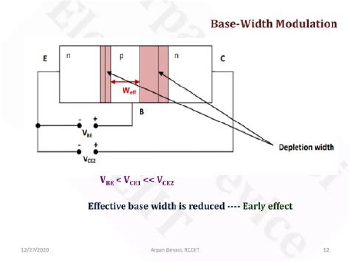
Answered Apr 6, 2018. #Base width modulation/Early effect is basically the variation in the width of the base in a bipolar transistor due to a variation in the applied base-to-collector voltage. #For example a greater reverse bias across the collector-base junction increases the collector-base depletion width..
Similarly one may ask, what is base modulation?
base modulation. [′bās ‚mäj·?′lā·sh?n] (electronics) Amplitude modulation produced by applying the modulating voltage to the base of a transistor amplifier.
Furthermore, what is base narrowing in BJT? In a BJT, if we change the reverse biasing voltage from collector to base junction, the depletion width changes which results in change in effective base width accordingly. This is known as base width modulation.
Additionally, what is base narrowing?
Base-narrowing has two consequences that affect the current: There is a lesser chance for recombination within the "smaller" base region. The charge gradient is increased across the base, and consequently, the current of minority carriers injected across the emitter junction increases.
What do you mean by early effect?
The Early effect, named after its discoverer James M. Early, is the variation in the effective width of the base in a bipolar junction transistor (BJT) due to a variation in the applied base-to-collector voltage.
Related Question Answers
How am wave is detected?
AM Detector. The detection of AM radio signals is a diode application. The modulated AM carrier wave is received by the antenna of the radio receiver and is rectified by the action of a detector diode. The signal frequency which modulates it is much lower, 0.02 to 5 kHz, and it can pass through the filter.Why is base made thin?
The Base region is thin so that the majority charge carriers coming from emitter find themselves near the Base collector junction and move to collector instead of going to Base terminal. It is lightly doped so that the depletion region is thin, electric field is strong and the resistance is small.Why is base width small?
The width of the base region is kept very small so that most the injected charge carriers pass to the collector. A transistor is basically a Si on Ge crystal containing three separate regions. In most transistors, emitter is heavily doped. Its job is to emit or inject electrons into the base.What are the types of AM modulators?
Types of Amplitude modulation: - Double Sideband Suppressed Carrier(DSB SC)
- Double side-band full carrier (Traditional Amplitude Modulation)
- Quadrature Amplitude Modulation (QAM)
- Single sideband (SSB)
- Vestigial sideband (VSB)
What is collector modulator?
Collector Modulator The tuned circuit, therefore, reproduces the negative portion of the carrier signal. The modulator is a linear power amplifier that takes the low level modulating signal and amplifies it to a high power level.What do you mean by base width modulation in BJT?
#Base width modulation/Early effect is basically the variation in the width of the base in a bipolar transistor due to a variation in the applied base-to-collector voltage. #For example a greater reverse bias across the collector-base junction increases the collector-base depletion width.What is the difference between BJT and FET?
BJTS and FETs can be used as switches and amplifiers in electrical and electronics circuits. The major difference between BJT and FET is that, in a field effect transistor only majority charge carries flows, whereas in BJT both majority and minority charge carriers flows.What is difference between NPN and PNP transistor?
The main difference between the NPN and PNP transistor is, an NPN transistor turns on when the current flows through the base of the transistor. In this type of transistor, the current flows from the collector (C) to the emitter (E). A PNP transistor turns ON, when there is no current at the base of the transistor.What are the applications of CE configuration?
Applications Of CE Amplifier The common emitter circuit is popular because it's well-suited for voltage amplification, especially at low frequencies. Common-emitter amplifiers are also used in radio frequency transceiver circuits. Common emitter configuration commonly used in low-noise amplifiers.How do you find early voltage?
The Early voltage, VA, is obtained by drawing a line tangential to the transistor I-V characteristic at the point of interest. The Early voltage equals the horizontal distance between the point chosen on the I-V characteristics and the intersection between the tangential line and the horizontal axis.Why BJT is called current controlled device?
A MOSFET is known as a voltage controlled device because a voltage applied to the gate controls the flow of current between the source and drain. For a BJT the principal is the same. It is a current controlled device because the base current controls the current flow from the emitter to collector.What are the consequences of early effect?
consequences of Early effect The increase in emitter current in turn causes a increase in the collector current. Also as effective base width decreases there is less chance for recombination and base current decreases as reverse bias increases. The base current is recombination current.What is Ebers Moll model?
Ebers Moll model is a simple and elegant way of representing the transistor as a circuit model. The Ebers Moll model of transistor holds for all regions of operation of transistor. This model is based on assumption that base spreading resistance can be neglected.What is punch through voltage?
punch-through voltage (VPT) The reverse-bias voltage applied to the drain terminal that results in significant drain-to-source current even though the transistor is biased in its off state.What is depletion region in pn junction?
Depletion region or depletion layer is a region in a P-N junction diode where no mobile charge carriers are present. Depletion layer acts like a barrier that opposes the flow of electrons from n-side and holes from p-side.What is meant by Q Point?
Q-Point. The operating point of a device, also known as a bias point, quiescent point or Q-point, is the steady-state DC voltage or current at a specified terminal of an active device such as a transistor with no input signal applied.What is the purpose of a BJT?
The main basic function of a BJT is to amplify current it will allow BJTs are used as amplifiers or switches to produce wide applicability in electronic equipment include mobile phones, industrial control, television, and radio transmitters. There are two different types of BJTs are available, they are NPN and PNP.What is stability factor?
Stability Factor (S): It is defined as the rate of change of collector current IC with respect to the collector base leakage current ICO, keeping both the current IB and the current gain β constant.Why FET is called voltage operated device?
A FET is voltage controlled device because its output characteristics are determined by the Field which depends on Voltage applied.